Doping organic semiconductor materials is a common practice to eliminate injection barriers at metal electrodes: Charge transfer from dopant molecules to the host material generates charge carriers that exit the material at the electrode. The leftover ion-charge induces an interface dipole which leads to fermi-level alignment between electrode and organic material. In addition to reducing injection, free charges from activated host-dopant pairs increase conductivity in injection layers.
Optimal performance of DILs depends strongly on activation and charge separation processes as well as injection into adjacent layers. Design of DIL materials therefore requires careful alignment of of host and dopant materials in the DIL, as well as materials in adjacent transport layers. To enable the efficient exploration of the chemical space of host-dopant combinations we developed a simulation approach that models doping processes on a microscopic level, to predict DIL performance in specific setups. In this approach we follow a multiscale simulation workflow to compute material- and state-specific rates for all microscopic processes involved, especially doping activation and charge transport, and apply kinetic Monte-Carlo (kMC) to simulate charge carrier dynamics of DILs and adjacent layers.
We apply this simulation protocol to a system containing NPB as both host and transport layer and F4TCNQ as dopant. We conduct simulations for a setup that was investigated experimentally and validate our simulation results against experimental data from literature. Ultimately we demonstrate how to apply this simulation approach to optimize DILs, specifically the dopant concentration.
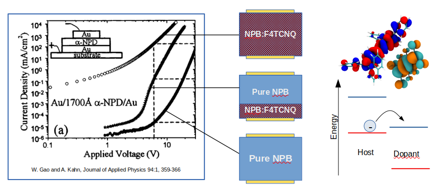
The figure below depicts experimental data from Gao et al. [1] (left) in combination with the device setups, namely (i) pristine NPB films, (ii) an NPB:F4TCNQ DIL with a pristine NPB transport layer and (iii) a single organic layer of NPB:F4TCNQ. The right panel of the figure below illustrates the microscopic doping process, an electron transferred from (neutral) host to the dopant.
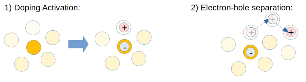
To simulate charge carrier dynamics in DILs on a microscopic level we need to consider two processes, illustrated below: (i) doping activation, i.e. the charge transfer between dopant and host material generating a hole-electron pair located on a host and a dopant moecule respectively (ii) the dynamic separation of the hole from the electron by hopping transport between host molecules.
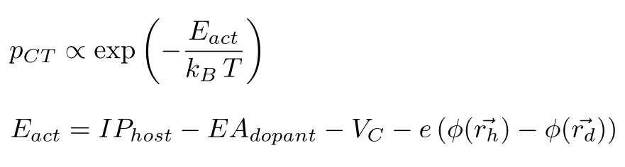
For each host-dopant pair in the system, the rate of the doping activation process depends on transport energy levels of host (IPhost) and dopants (EAdopant), as well as the coulomb binding energy VC of an activated host-dopant pair and the electrostatic potential on each molecule depending on the charge distribution in the system:
To compute IP, EA and VC we follow our typical workflow and generate a mixed morphology of 2000-3000 molecules. With QuantumPatch we run a full quantum mechanical electronic structure analysis of molecules in the thin film taking into account their unique electrostatic environment as well as the polarization response of surrounding molecules to charges. Distributions of IP and EA are then computed by subtracting total energies of charged and neutral state of multiple molecules the morphology. VC is computed for various pairs in the morphology via a partial-charge based estimator. The electron-hole separation is modeled by hopping transport based on Marcus-like rates, which require electronic couplings in addition to distributions of site energies (IP or EA) also computed in QuantumPatch.
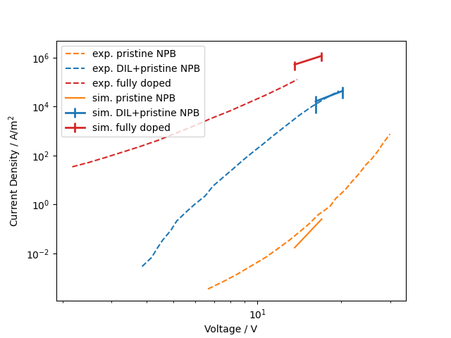
Based on morphologies and distributions of all microscopic quantities from QuantumPatch we generate expanded systems of 14x14x40nm³ organic thin film embedded between Au-electrodes in LightForge and conduct charge carrier simulations at constant fields to compute current-voltage characteristics of all three test systems (pristine NPB, NPB:F4TCNQ combined with a pristine NPB layer, and a single layer of NPB:F4TCNQ). The figure below depicts simulated I-V in comparison to experimental data from Gao et al. [1]. The applied voltage (x-axis) was adjusted to account for the reduced layer thicknesses in comparison to experiment. For all three systems we find good agreement between simulation and experiment, thereby validating the microscopic model to simulate doping activation and charge transport in DILs.
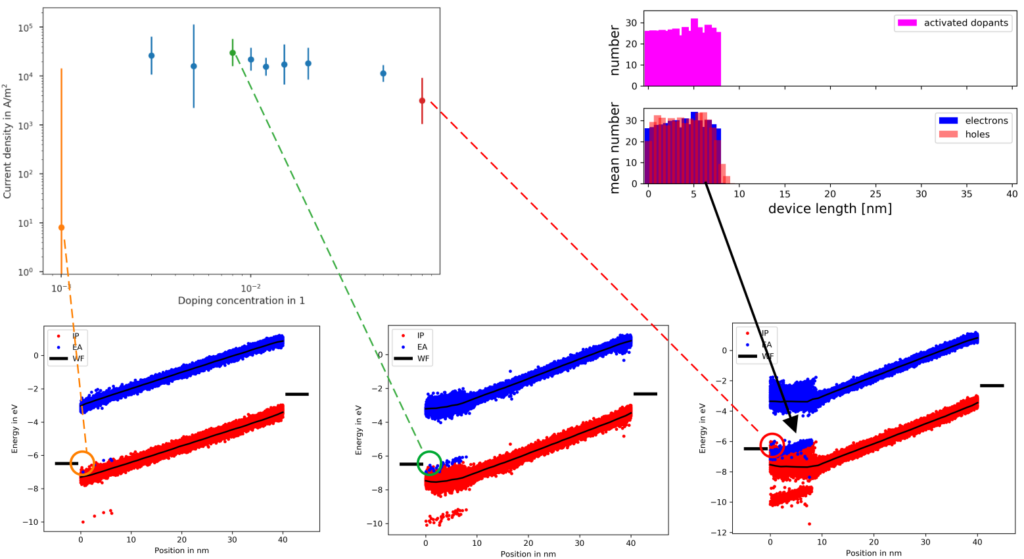
In order to illustrate how this simulation approach can be used to aid experimental R&D and optimization of DIL setups, we simulated the system including both a doped DIL and a pristine transport layer at different dopant concentrations in the DIL. The figure below depicts current densities at dopant concentrations between 0.1% and 8%(mol), as well as snapshots of the band diagrams at 0.1%, 0.8% and 8%. The current density at 0.1% dopant concentration is more than three orders of magnitude below current densities at higher concentration. The corresponding band diagram shows that 0.1% dopant are insufficient to induce full fermi-level alignment at the electrode, resulting in a persisting injection barrier and therefore reduced conductivity. The 8% on the other hand system shows good fermi-level alignment at the electrode, but a current density below the 0.8%-system. Potential reasons are twofold: First, increased number of dopant molecules with a large quadrupole moment increases energy disorder in the DIL, resulting in a small, yet sufficiently significant injection barrier between (upper) tail states of DIL-host and adjacent transport layer, even though both are the same material (NPB). Further, as indicated by the charge distribution in the top right, at the interface between DIL and transport layer holes from the DIL diffuse into the transport layer, generating an interface dipole and therefore increasing the injection barrier at this interface.
In this study we applied our microscopic simulation workflow to systems including doped injection layers and validated ab-initio simulations against experimental data from literature. This workflow can therefore aid experimental R&D of DIL systems by identifying suitable material combinations, as well as optimizing system parameters such as dopant concentrations.
References:
[1] Gao et al., J. Appl. Phys., Vol. 94, No. 1, 1 July 2003